10th International Symposium on Dielectric Materials and Applications (ISyDMA’10)
Technical University of Moldova, Chișinău, Moldova
About the Conference
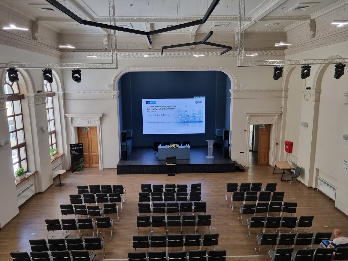
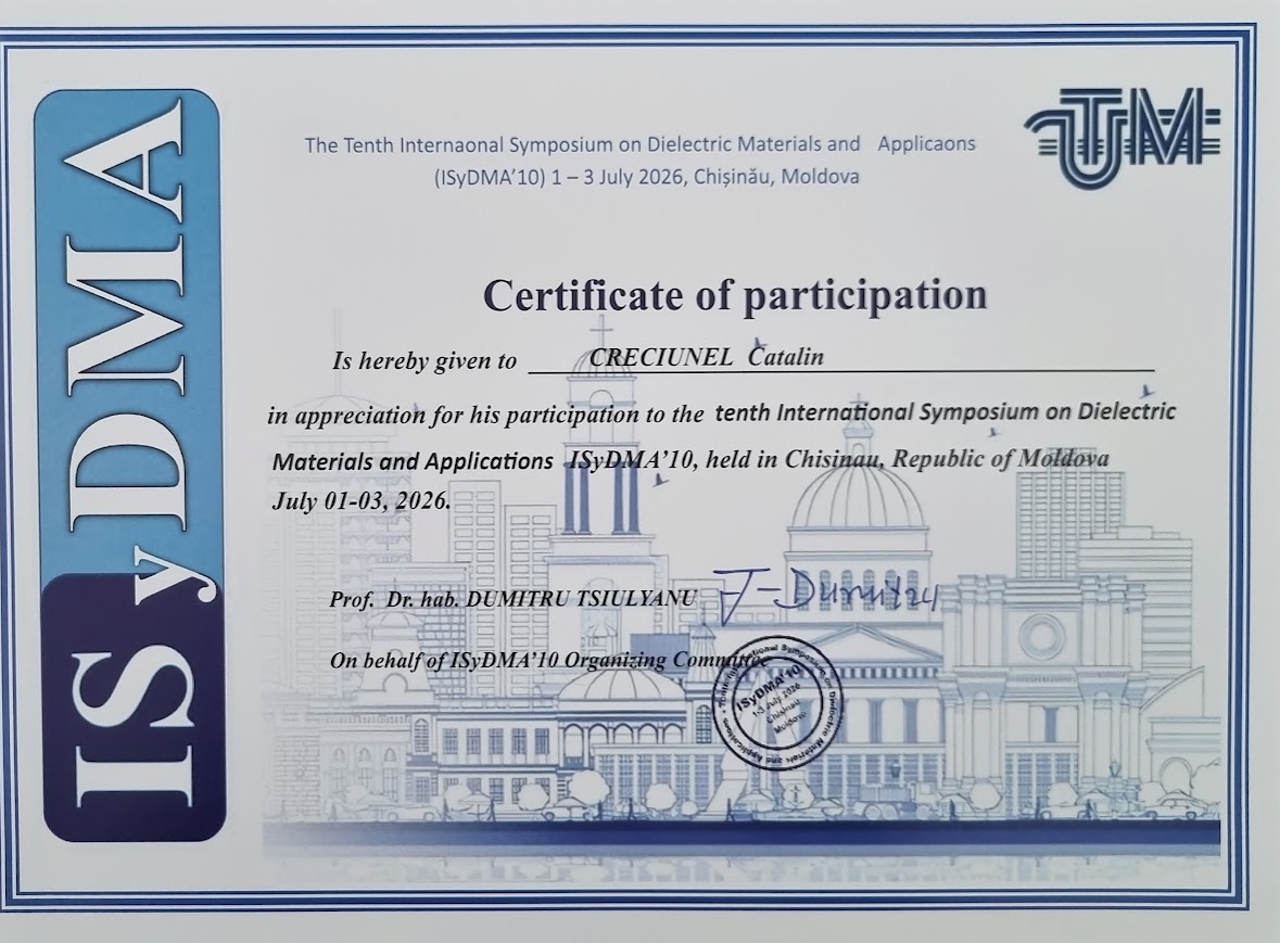
The 10th International Symposium on Dielectric Materials and Applications (ISyDMA’10) was hosted in Chișinău, Republic of Moldova, during July 1–3, 2026, organized by the Technical University of Moldova.
As a premier international event, ISyDMA’10 focused on recent developments in dielectric materials and their cutting-edge applications. The symposium brought together over 150 leading scientists, physicists, chemists, and engineers from more than 25 nationalities to discuss advanced materials optimized for biomedical, biotechnological, and industrial fields. All accepted peer-reviewed works from the meeting are published in the official Conference Proceedings by Springer Nature.
Official Video Introduction
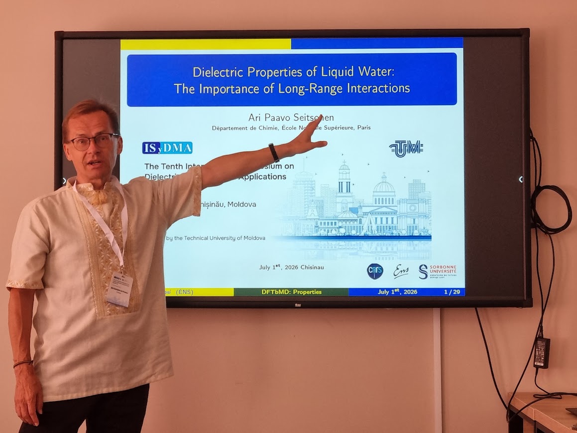
Notable Keynote & Invited Speakers
The conference featured an elite lineup of global researchers. Among the most distinguished scientists who delivered keynote lectures were:
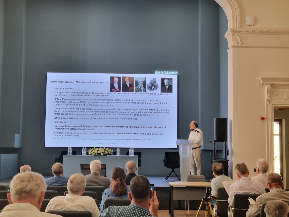
- Prof. Christian Brosseau (Université de Bretagne Occidentale, France) – Presenting groundbreaking work on the “Electromagnetism of Functional Biomaterials”.
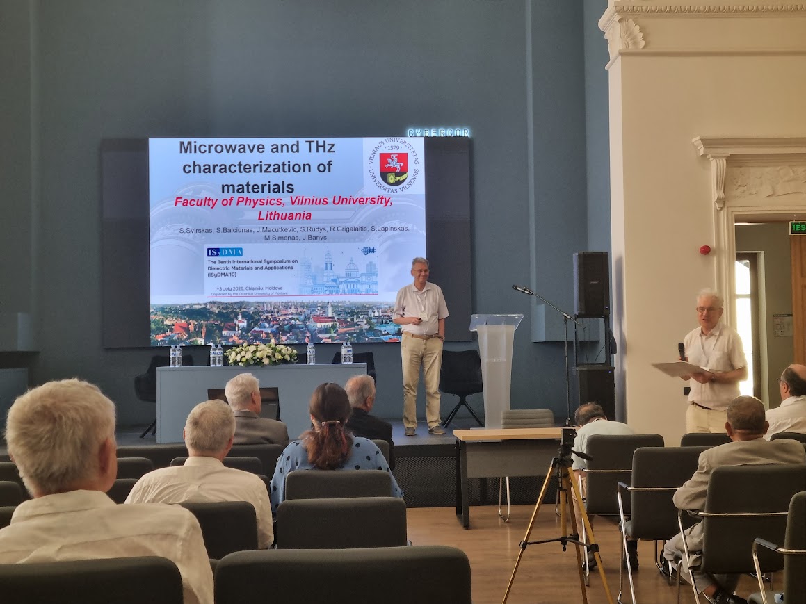
- Prof. Juras Banys (Vilnius University, Lithuania) – A pioneer in core dielectric physics, discussing “Broadband frequency measurements of advanced materials”.
- Prof. Yasuo Cho (Tohoku University, Japan) – Highlighting next-generation data systems in “Recent progress on R&D for practical application of HDD-type ultra-high density ferroelectric data storage”.
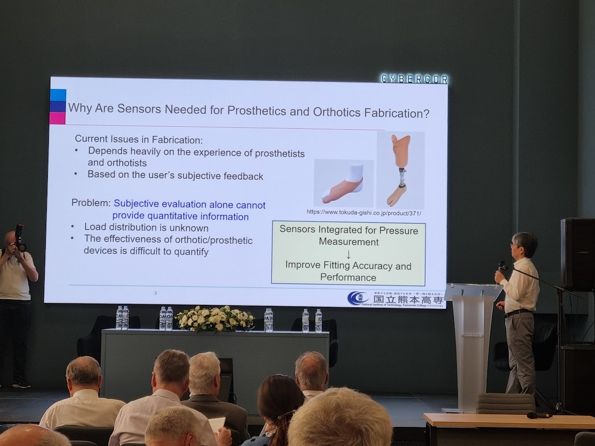
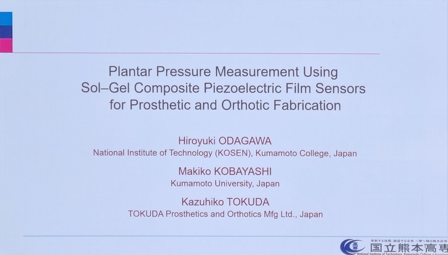
- Prof. Hiroyuki Odagawa (National Institute of Technology, Koshi, Japan) – Unveiling innovative applications in “Plantar Pressure Measurement Using Sol–Gel Composite Piezoelectric Film Sensors for Prosthetic and Orthotic Fabrication”.
Key Speakers & Venue
My Contribution & Research Focus
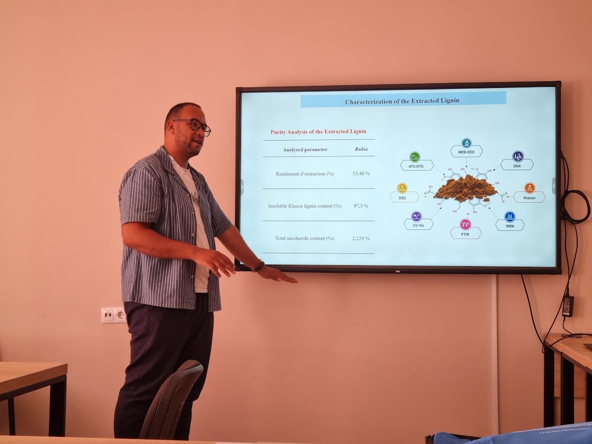
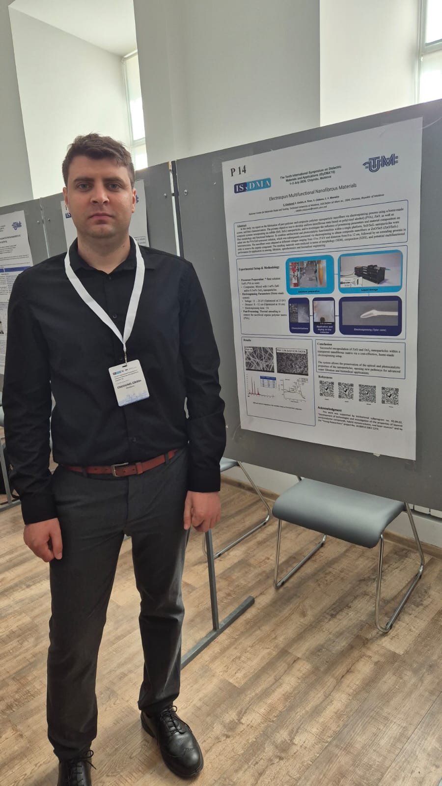
I had the opportunity to present our latest team research from the National Center for Materials Study and Testing (NCMST) focused on advanced nanotechnology fabrication loops.
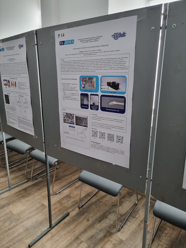
ELECTROSPUN MULTIFUNCTIONAL NANOFIBROUS MATERIALS
C. Creciunel*, C. Cechin, A. Tiron, V. Ciobanu, E.V. Monaico
National Center for Materials Study and Testing, Technical University of Moldova, Chisinau, Republic of Moldova
*Email: catalin.creciunel@cnstm.utm.md
Abstract: Electrospinning is a versatile and widely employed technique for the fabrication of nanofibrous polymeric or semiconductor materials with controlled morphology, high surface-to-volume ratio, and tunable functional properties. $\text{ZnO}$ nanofibers fabricated by this method are widely investigated due to the material properties such as electrical, optical, or antibacterial activity, making it suitable for multifunctional applications. Besides $\text{ZnO}$, tin sulfide-based materials, including $\text{SnS}$ and $\text{SnS}_2$, have demonstrated promising performance in optoelectronic devices such as photodetectors as well as in photocatalytic processes, particularly in the case of $\text{SnS}_2$ due to its favorable electronic structure.
In this study, we report on the fabrication of pure polymer and composite polymer–nanoparticle nanofibers via electrospinning process using a home-made system, and their characterization. The primary objective was to develop uniform nanofibrous mats based on poly(vinyl alcohol) (PVA), $\text{ZnO}$, as well as composite systems incorporating tin sulfide ($\text{SnS}$, $\text{SnS}_2$) nanoparticles, and to investigate the influence of processing parameters and material composition on fiber morphology and functional behavior.
To combine antibacterial and photocatalytic functionalities within a single platform, $\text{SnS/SnS}_2$ nanoparticles were added into the $\text{PVA/ZnO}$ precursor solution, which was subsequently processed via electrospinning to obtain composite nanofibers or $\text{ZnO/SnS}$ ($\text{ZnO/SnS}_2$) heterostructures. The nanofibers were obtained at different voltages ranging from 15 to 25 kV and distances from 8 to 12 cm, followed by an annealing process in order to remove the organic compound. The resulting materials were analyzed in terms of morphology (SEM), composition (EDX), and potential multifunctional performance for application in sensing, filtration, optoelectronics and biomedical engineering.
Keywords: Electrospinning; nanofibers; composite materials; ZnO; chalcogenides
Technical Session & Program Overview
The presentations were highly collaborative, balancing complex materials physics with industrial scalability. You can track the timeline and structure of the event through the materials below:

Takeaways
The data gathered from our custom electrospinning configuration proves that tuning physical constraints like voltage and distance directly controls the resulting semiconductor matrix morphology. This creates real-world development options for high-efficiency sensors and localized medical filtration networks.
